
Author Affiliations
Abstract
1 Wuhan National Laboratory for Optoelectronics, Huazhong University of Science and Technology, Wuhan 430074, China
2 e-mail: dainl@hust.edu.cn
3 e-mail: ywangwnlo@mail.hust.edu.cn
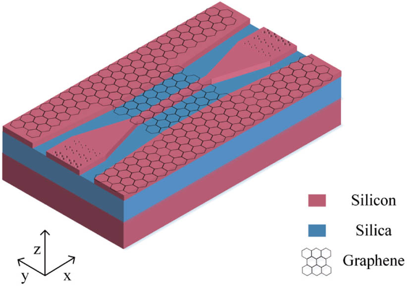
On-chip ultrafast mode-locking lasers are basic building blocks for the realization of a chip-based optical frequency comb. In this paper, an ultrafast saturable absorber made up of a graphene pad on top of a silicon waveguide is applied to implement an ultrafast pulse laser. Benefiting from the small mode area of the graphene/silicon hybrid waveguide, the saturable pulse energy is reduced by two orders of magnitude compared with the fiber. A mode-locked pulse with a duration of 542 fs and a repetition rate of 54.37 MHz is realized. Pump–probe measurement shows that the carrier relaxation process of free carrier recombination with atomic-thin graphene/silicon junctions is three orders of magnitude faster than silicon, which plays a fundamental role in pulse narrowing. The chip-scale silicon ultrafast laser lays a foundation for a new class of nonlinear devices, in which a combination with multiple functional silicon photonic circuits enables efficient nonlinear interaction at the micrometer scale and less than 1 W of power consumption.
Photonics Research
2021, 9(9): 09001660
Author Affiliations
Abstract
1 Wuhan National Laboratory for Optoelectronics, Huazhong University of Science and Technology, Wuhan 430074, China
2 Institute of Semiconductors, Chinese Academy of Sciences, Beijing 100038, China
3 e-mail: chizheung@hust.edu.cn
4 e-mail: lizhy@semi.ac.cn
Graphene resting on a silicon-on-insulator platform offers great potential for optoelectronic devices. In the paper, we demonstrate all-optical modulation on the graphene–silicon hybrid waveguides (GSHWs) with tens of micrometers in length. Owing to strong interaction between graphene and silicon strip waveguides with compact light confinement, the modulation depth reaches 22.7% with a saturation threshold down to 1.38 pJ per pulse and a 30-μm-long graphene pad. A response time of 1.65 ps is verified by a pump–probe measurement with an energy consumption of 2.1 pJ. The complementary metal-oxide semiconductor compatible GSHWs with the strip configuration exhibit great potential for ultrafast and broadband all-optical modulation, indicating that employing two-dimensional materials has become a complementary technology to promote the silicon photonic platform.
Photonics Research
2020, 8(4): 04000468
1 太原科技大学机械工程学院, 山西 太原 030024
2 浙江大学宁波理工学院机电与能源工程学院, 浙江 宁波 315100
采用正交实验优化了激光加工导轨试样的工艺参数,用光学显微镜、扫描电镜和显微硬度计对试样进行了显微组织分析和硬度测试,并在油润滑下与常规处理试样进行了磨损性能对比试验。结果显示,电流对硬化深度影响最显著,然后依次为扫描速度、脉宽和频率,优化后的激光加工参数:扫描速度为0.25 mm/s,电流为150 A,脉宽为10 ms,频率为7 Hz。激光加工试样熔凝区分布有球状石墨,相变区晶粒尺寸较熔凝区更细小,分布更均匀;硬度较常规处理有显著提高,其分布无变化梯度。当循环次数达38000时,激光加工试样较常规处理试样耐磨性提高约1倍。
激光技术 激光强化 导轨 参数优化 显微组织 显微硬度 耐磨性


